|
The silicon-based waveguide optical coupling technology is mainly used to solve the problem of interconnecting optical signals on silicon-based integrated optoelectronic chips with external optical signals, and is also a key technology for silicon-based optoelectronic chip packaging.
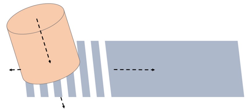
The width of the silicon-based optical waveguide is usually about 300 nm to 500 nm, which is a large difference in geometry compared to the commonly used single-mode optical fiber (the core diameter is about 8 to 10 um). The large difference in geometric size causes the mode field. Serious mismatch, as shown in Figure 1. By designing optical coupling devices of different structures and materials, the optical mode field of the on-chip silicon waveguide is matched with the optical mode field coupling of the single-mode fiber to achieve optimal optical coupling efficiency, usually using SSC (spot size converter) coupling and There are two ways of grating coupling. The waveguide end face coupler and grating coupler developed by the EPIC group have reached the world's leading level [1-2].
|
|
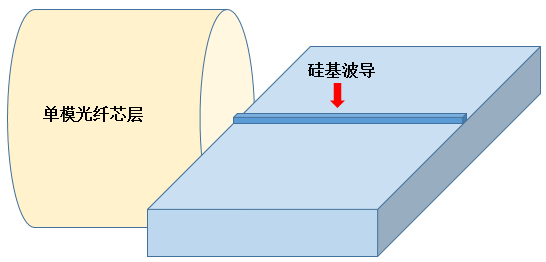 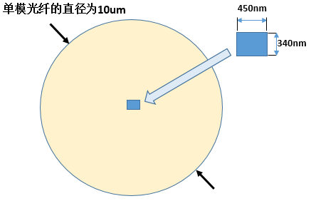
Figure 1: Schematic diagram of coupling of a single-mode fiber to a silicon waveguide
|
|
SSC mode spot converter
End face coupling is achieved by applying an end face coupler, which helps the optical signal directly coupled to the cross section of the silicon based waveguide and the cross section of the optical fiber. The advantage of the end face coupler is that the coupling efficiency is high and alignment can be performed without changing the optical path. In the preparation process, the process is difficult, the manufacturing tolerance is small, and special end face polishing is required.
The mode field of light wave propagation is changed by fabricating a multilayer waveguide structure on the end face of the silicon waveguide to achieve matching of different diameter mode fields, as shown in FIG. 2 . Different waveguide materials and external dimensions have a great influence on the SSC coupling loss.
Foreign research institutions such as NTT, Intel, Bell Lab, etc. have reported related research on SSC couplers. In 2008, Intel reported a double-layer forward taper coupler with a coupling loss of 1.5dB/port [3]. In 2010, Bell Labs reported a cantilever structure SSC. In the 1550 nm band, the coupling loss of TE mode light waves is about 0.8 dB, and the coupling loss of TM mode light waves is about 1 dB [4].
By using FDTD, BPM simulation software and multiple explorations of the device fabrication process, we fabricated a reverse wedge die spot converter. When the 1550nm wavelength is coupled with the MFD=4um fiber, the TE mode has a coupling loss of 0.62dB, the TM mode has a coupling loss of 0.95dB, and the 1dB bandwidth reaches 100nm. In the C-band and L-band, the average coupling loss of the TE mode is about 1 dB, and the average coupling loss of the TM mode is about 1.3 dB. [1]
|
|
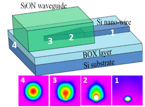 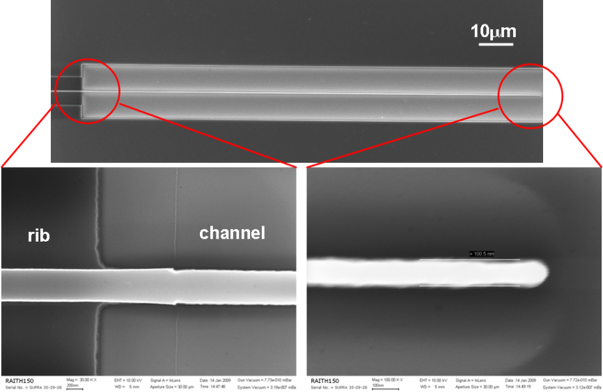
(a) Optical mode field transformation in SSC mode spot converter (b) SEM image of mode spot converter
Figure 2: Schematic diagram of SSC working principle
|
|
|
|
Grating coupler
The grating coupler is a common coupler that realizes the optical interconnection between the chip and the optical fiber. The schematic diagram of the grating coupling mode is shown in Fig. 3(a), and the direction of the optical fiber is vertical (or slightly deviated) to the grating coupler. When light is incident from the fiber to the grating coupler surface, the diffracted light will be mutually interfered in the direction perpendicular to the grating structure due to the Bragg diffraction effect, thereby allowing a portion of the optical grating coupler to enter the optical waveguide in the chip. In this way, the design of the coupler structure and position is more free, and the size of the grating structure (usually 12um x 12um) is compatible with the size of the fiber core (8~10um), which can improve the pair Quasi-tolerance of fiber and coupler.
|
|
(a)
Figure 3: Schematic diagram of the grating coupler
|
|
In 2002, the Ghent University of Belgium first developed a grating coupler on GaAs-AlOx with a coupling efficiency of 19% [5]. In 2009, Hamburg-Hamburg University of Technology produced a grating coupler with a one-step process step on the SOI substrate, with a coupling efficiency of 49% [6].
The EPIC group designed and fabricated a gradual-period grating coupler [2] and a uniform-period grating coupler on the SOI substrate. The variable-cycle grating coupling efficiency reached -0.85dB, 3dB bandwidth 55nm, and uniform period grating coupling efficiency. It has reached -4dB and the 3dB bandwidth is 60nm, which has reached world-class level.
|
|
|
|
Array coupling
Array coupling is an important form of multi-channel optical device interaction with the outside. Due to the simultaneous multi-port coupling, the coupling error of the port will accumulate, which is more difficult than single-port coupling. And it can be divided into grating array coupling and end-face SSC array coupling. Grating array coupling is a common array coupling form of optoelectronic chips. It has the advantages of simple operation and large alignment tolerance. It is a common coupling method for product packaging and device testing. The end face SSC array coupling will be the main form of future optoelectronic device packaging due to its small loss and small package size. The EPIC group has actively explored array coupling and has achieved certain research results.
In summary, the coupling between a standard single-mode fiber array and a silicon-based waveguide array will be an important means to solve the problem of large-scale, high-density integrated silicon photonic chips and external optical interconnects in the future.
|
|
|
|
Biliography:
[1] Y. Fu, Z. Li, T. Chu, Y. Yu, J. Yu, and Q. Li: “Broad-band Efficient Edge Couplers for Compact Silicon Photonic Circuits”, Information Optoelectronics, Nanofabrication and Testing, OSA Technical Digest (online) (Optical Society of America),(2012);
[2] C. Zhang, J. Sun, X. Xiao, W. Sun, X. Zhang, T. Chu, J. Yu, Y. YU: “High Efficiency Grating Coupler for Coupling between Single-Mode Fiber and SOI Waveguides”, Chinese Physics Letter, 30, 1, pp.014207-1-4, (2013);
[3] Barkai A, Liu A, Kim D, et al. “Double-stage taper for coupling between SOI waveguides and single-mode fiber”. Journal of Lightwave Technology, 2008, 26(24): 3860-3865.(2008);
[4] Chen L, Doerr C R, Chen Y K, et al.” Low-Loss and Broadband Cantilever Couplers Between Standard Cleaved Fibers and High-Index-Contrast Si< formula formulatype”. Photonics Technology Letters, IEEE, 22(23): 1744-1746.(2010);
[5] Taillaert, D.; Bogaerts, W.; Bienstman, P.; Krauss, T.F.; van Daele, P.; Moerman, I.; Verstuyft, S.; De Mesel, K.; Baets, R., "An out-of-plane grating coupler for efficient butt-coupling between compact planar waveguides and single-mode fibers," Quantum Electronics, IEEE Journal of 2002, vol.38, no.7, pp.949,955,(2002);
[6] Bernd Schmid, Alexander Petrov, and Manfred Eich, "Optimized grating coupler with fully etched slots," Opt. Express 17, 11066-11076 (2009);
|
|